
Hybrid Bonding, Fully Dissected
The Technology Deciding AI's Next Bottleneck

If you had to name the single hottest keyword in the semiconductor industry right now, I’d say hybrid bonding without hesitation.
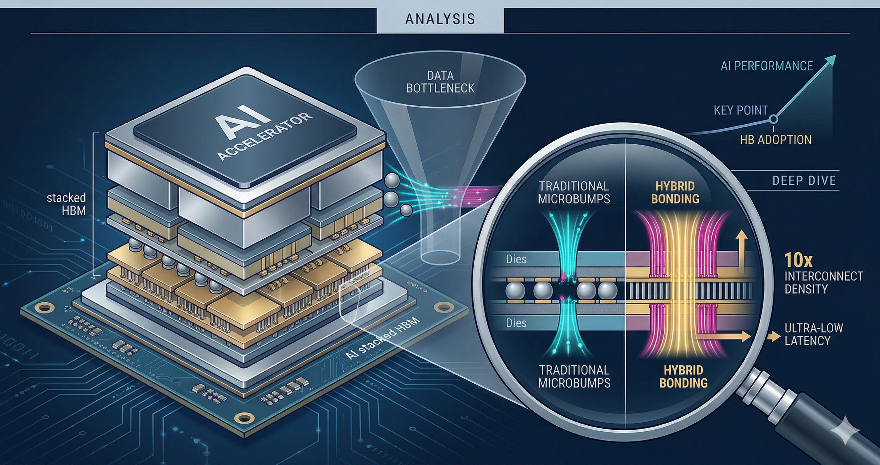
EUV lithography was the revolution that shrank transistors horizontally. Hybrid bonding is the revolution that stacks chips vertically. As transistor scaling approaches its physical limits, the path to higher performance is no longer about making chips smaller: it's about stacking multiple chips in three dimensions and making them behave as one. Hybrid bonding is the core technology that makes that 3D integration possible.
For this article, I conducted direct interviews with engineers currently working at Samsung, SK Hynix, and Micron. This piece covers what hybrid bonding is, how it differs across applications, why it's uniquely difficult for HBM, whether it will actually be adopted, and who the beneficiaries are.
Table of Contents
1. What Is Hybrid Bonding
2. Bonding Methods: W2W, D2W, and D2D
3. Where Hybrid Bonding Is Applied, and Why Some Are Harder Than Others
4. Why HBM Hybrid Bonding Is So Much Harder
5. Will HBM Actually Use Hybrid Bonding?
6. Beneficiary Analysis: Who Makes the Money
1. What Is Hybrid Bonding
The old way: bumps
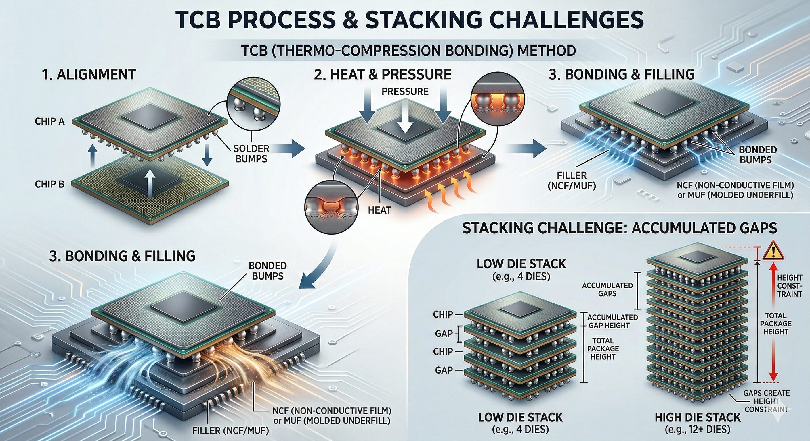
The most traditional method for connecting chip to chip is the bump. A bump is a tiny solder ball that protrudes from the chip surface. You align the bumps on chip A with the bumps on chip B, apply heat and pressure, the solder melts, and the two chips form an electrical connection.
TCB (Thermo-Compression Bonding), currently the dominant method in HBM, works exactly this way. A filler material, either NCF (Non-Conductive Film) or MUF (Molded Underfill), is injected between chips to fill the gaps around the bumps. SK Hynix's MR-MUF (Mass Reflow Molded Underfill) is the best-in-class implementation of this approach.
The problem is that bumps take up space. If the bump pitch (center-to-center distance between bumps) is 40μm, there is an unavoidable gap of tens of microns between chips. That’s fine when you’re stacking four dies. When you need to stack 12, 16, or eventually 20, those accumulated gaps become a hard constraint on total package height.
Hybrid bonding: eliminate the bump
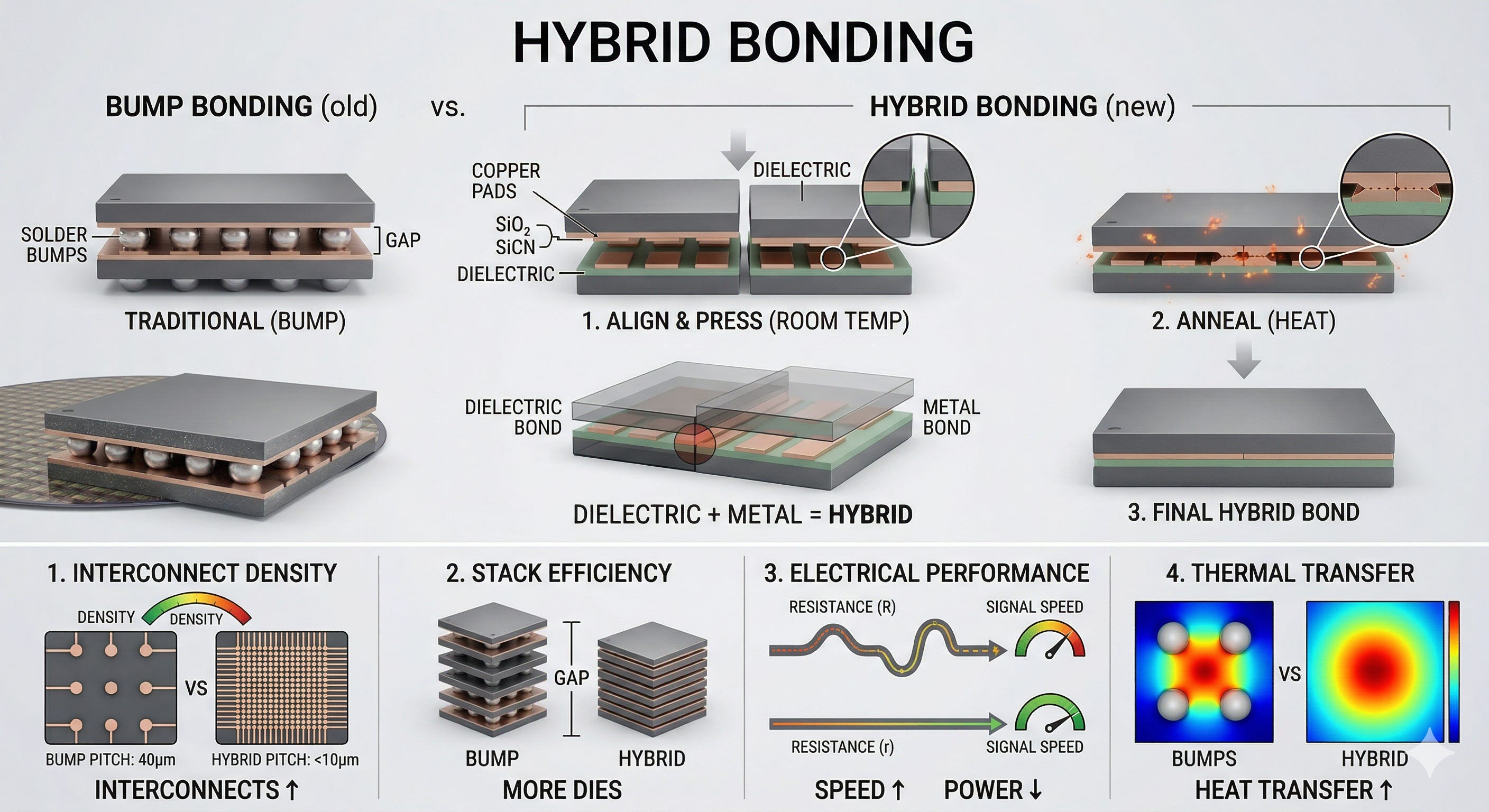
Hybrid bonding removes bumps entirely. Instead of a solder ball, the chip surface exposes bare copper pads surrounded by a dielectric (SiO₂ or SiCN). When two chips are pressed face-to-face, the dielectrics bond first at room temperature or low temperature. A subsequent annealing step heats the assembly, causing the copper pads to expand thermally and form a direct metal-to-metal bond.
Why “hybrid”?
Because dielectric bonding and metal bonding happen simultaneously. It’s not purely copper bonding, and it’s not purely dielectric bonding. The two mechanisms work in tandem.
What that actually means:
First, no bumps means virtually zero gap between chips. You can fit more dies within the same total height. Second, bump pitch was 40μm; with hybrid bonding it can drop below 10μm, and ultimately to sub-micron. Interconnect density goes up by orders of magnitude. Third, removing the bump as an intermediary lowers electrical resistance, speeds up signal transmission, and reduces power consumption. Fourth, bumps were a thermal bottleneck between chips; hybrid bonding also improves heat transfer across the die-to-die interface.
In short: hybrid bonding enables 3D stacking that is denser, faster, more interconnect-rich, and thermally superior.
Pitch: what it is, and why it matters
Earlier I said bump pitch goes from 40μm down to below 10μm. Here’s what that actually means.
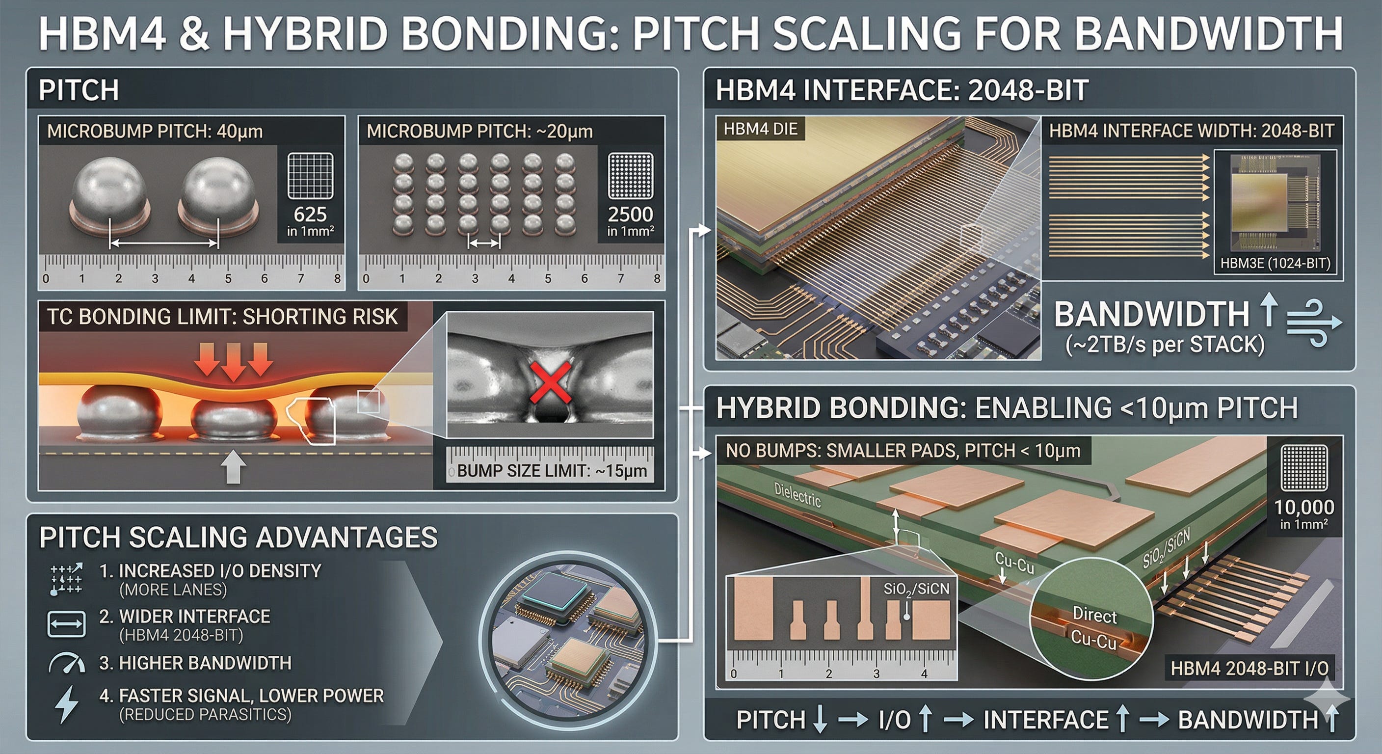
Pitch is the center-to-center distance between adjacent connection points. Think of a grid: the spacing between intersections is the pitch. The tighter the spacing, the more connection points you can fit in a given area.
The numbers tell the story. At 40μm pitch, you can fit 25 connection points along a 1mm line. Extend that to a 1mm × 1mm area and you get roughly 625 total connections. At 10μm pitch? 100 per millimeter, 10,000 per square millimeter. Cut the pitch by 4x and interconnect density jumps 16x. Push hybrid bonding to 1μm pitch and you get one million connections per square millimeter — 1,600x the density of a 40μm bump.
Why does this matter for HBM? The HBM4 interface is 2,048 bits wide, double the 1,024 bits of HBM3E. Bit count is the number of “lanes” available to send and receive data simultaneously. More lanes means higher bandwidth. HBM4’s per-stack bandwidth of 2TB/s comes directly from that wider interface.
The challenge is fitting 2,048+ I/O pins into the physical footprint of an HBM die. The area is limited. At 40μm pitch, you simply cannot pack that many I/Os into the available space. HBM4 already requires pitch to be pushed well below 40μm, and future generations will need to approach 10μm. At that point, bump-based TC Bonding hits a wall — the physical size of the bump itself is the bottleneck.
Hybrid bonding solves this at the root. Copper pads sit flush with the chip surface rather than protruding, so the pads themselves can be made much smaller. Smaller pads mean tighter pitch, which means more I/Os in the same area. Below 10μm pitch, you can fit tens of thousands of connection points — more than enough to support 2,048 bits and beyond.
The chain of logic: tighter pitch → more connections per unit area → wider interface → higher bandwidth. HBM bandwidth requirements are growing explosively with each generation. The physical foundation for that bandwidth is pitch. Hybrid bonding is what breaks through the physical limits on pitch.
One more thing. Tighter pitch doesn’t just add connection density. Shorter interconnect paths reduce parasitic capacitance and inductance, which speeds up signal transmission and lowers power consumption. HBM4’s per-pin data rate of 8Gb/s is built on exactly these physical improvements.
The non-negotiable prerequisite: atomic-level surface flatness
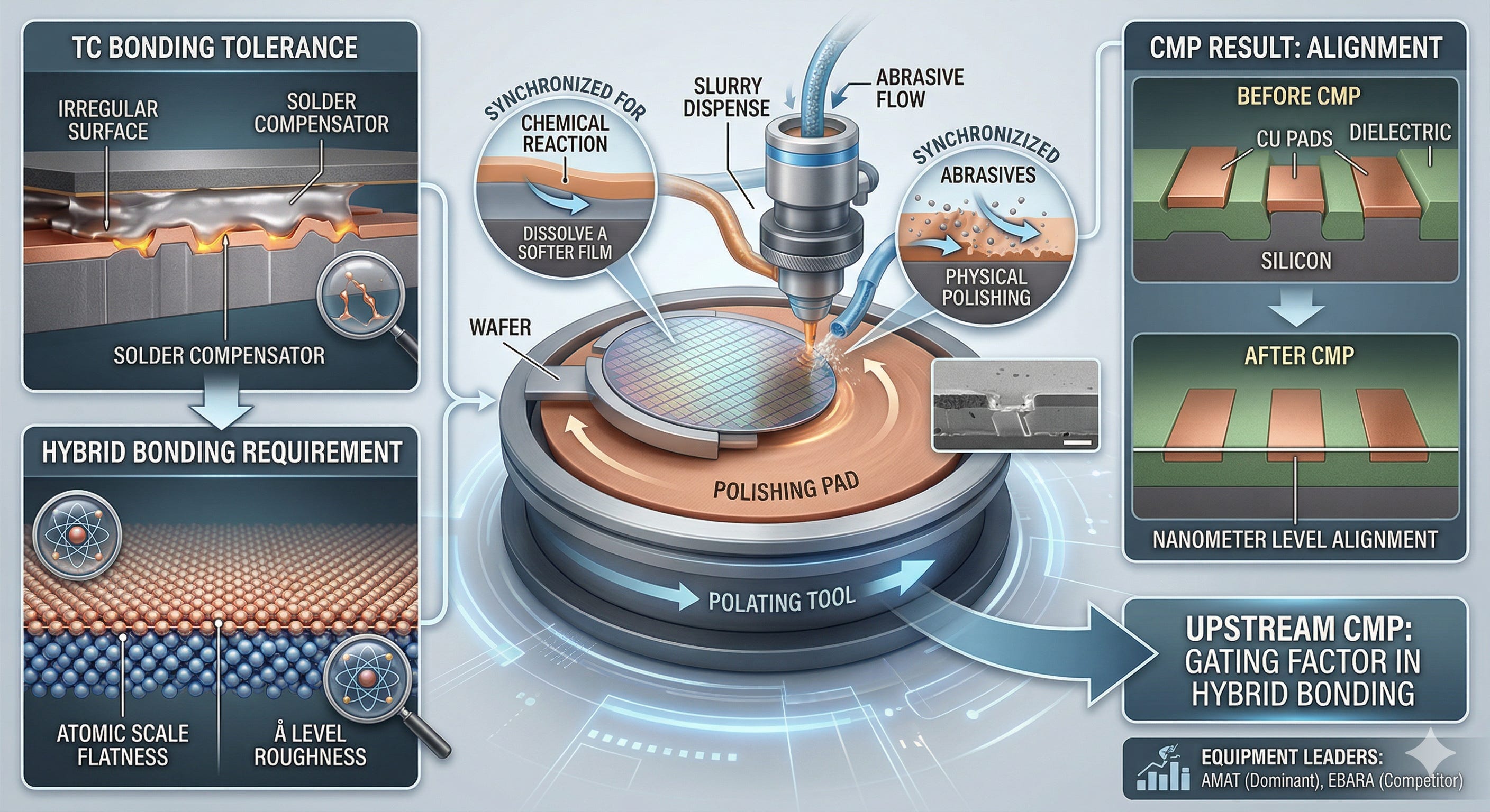
For hybrid bonding to work, chip surfaces must be flat at the atomic scale. TC Bonding can tolerate surface irregularity because molten solder compensates for height variations. Hybrid bonding has no such buffer. Surface roughness must be on the order of a few angstroms (1Å = 0.1nm).
The process that achieves this flatness is CMP (Chemical Mechanical Planarization). CMP combines chemical reaction and physical polishing to bring copper pad height and surrounding dielectric height into alignment at the nanometer level. Applied Materials (AMAT) holds a dominant position in the CMP equipment market for hybrid bonding applications. Competitors like Japan’s EBARA exist, but AMAT’s technical lead in hybrid bonding-specific CMP is firmly established. The fact that the real gating factor in hybrid bonding is not the bonder itself but the upstream CMP process will come up again when we get to the beneficiary analysis.
2. Bonding Methods: W2W, D2W, and D2D
Before getting into the Hybrid bonding applications, it helps to understand the three primary bonding methods. W2W, D2W, and D2D are not concepts unique to hybrid bonding; they apply to bonding broadly. But in practice, they come up far more often in the hybrid bonding context. The reason is that hybrid bonding is extremely sensitive to alignment error, particle contamination, and yield loss, which means the choice of assembly format has an outsized impact on both yield and cost.
The Three Methods: W2W, D2W, and D2D
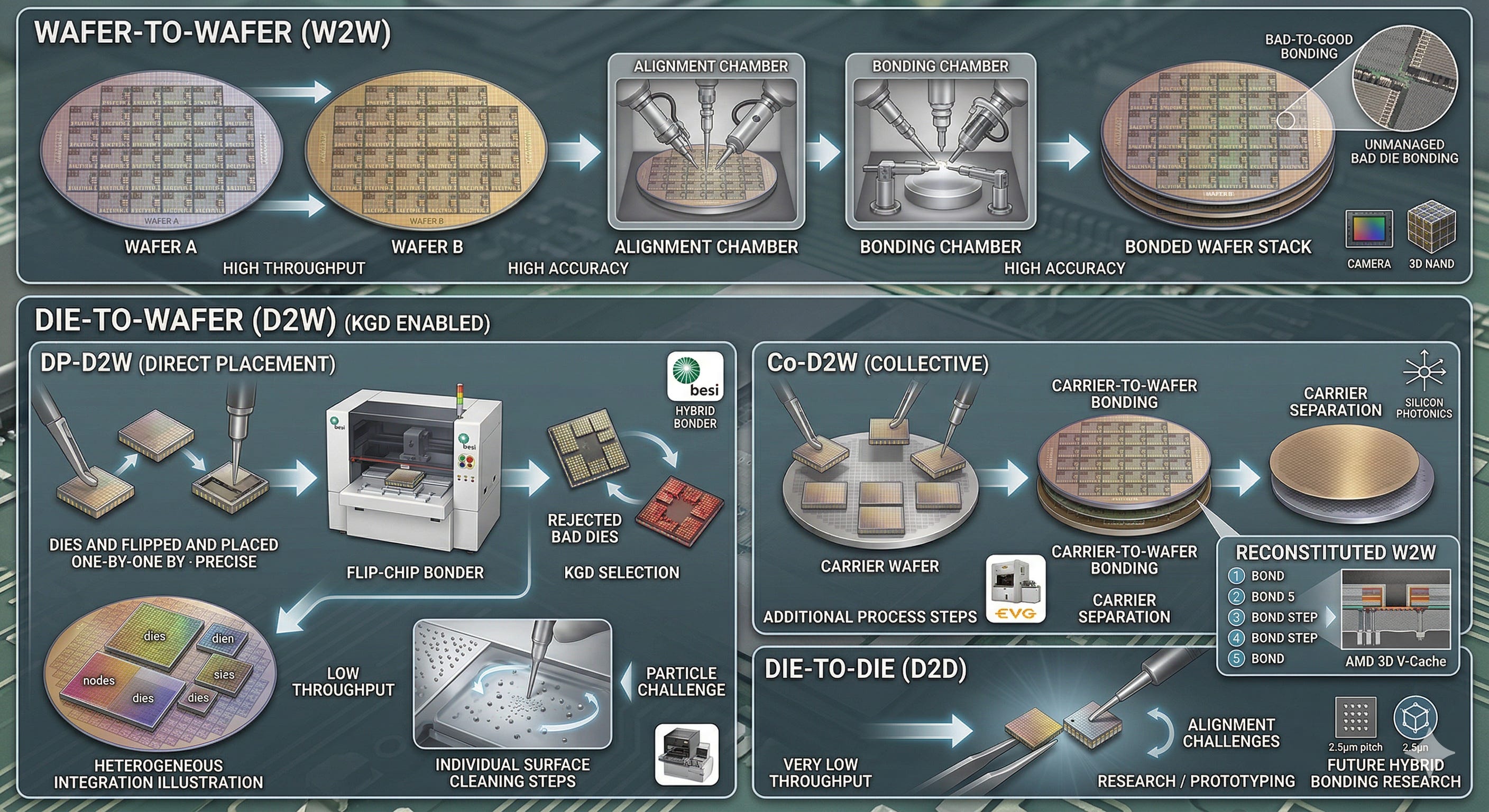
W2W (Wafer-to-Wafer)
Two fully fabricated wafers are aligned and bonded face-to-face as complete units. Alignment and bonding occur in separate chambers, which is why this method delivers the highest alignment accuracy, throughput, and bond yield of the three.
The constraint is that both wafers must have identically sized dies, which rules out heterogeneous integration. And because entire wafers are bonded at once, there’s no opportunity to screen out defective dies beforehand. W2W works best for small, high-yield chips where the yield loss from bonding a bad die to a good one is manageable.
Applications: Sony CIS, YMTC Xtacking (3D NAND), Micro-LED microdisplays, 3D DRAM CBA.
D2W (Die-to-Wafer)
Individual dies are placed and bonded onto a target wafer. This enables KGD (Known Good Die) selection and allows dies of different sizes, thicknesses, and process nodes to be combined on a single wafer, making it the method of choice for heterogeneous integration. D2W splits into two distinct sub-approaches.
DP-D2W (Direct Placement D2W): Individual dies are picked, flipped, and placed directly onto the target wafer one at a time using a high-precision flip-chip bonder. Maximum flexibility for mixing different die types, but the lowest throughput of the D2W approaches. Each die requires individual surface cleaning and activation, which makes particle control a persistent challenge. Besi’s hybrid bonder is the leading equipment platform for this method.
Applications: HBM stacking (future generations), select TSMC SoIC configurations.
Co-D2W (Collective D2W): Individual dies are first placed onto a carrier wafer, then the carrier and target wafer are bonded together in a single W2W-like step. This improves throughput over DP-D2W and partially inherits W2W alignment advantages, but adds process steps for carrier preparation, temporary bonding, and carrier separation. EVG is the key equipment supplier for this approach.
Applications: Silicon photonics, TSMC SoIC (reconstituted method).
A notable variant here is Reconstituted W2W, used in TSMC’s SoIC platform. Dies for both the top and bottom layers are individually placed onto separate carrier wafers, and the two carriers are then bonded W2W. AMD’s 3D V-Cache is built this way. A single V-Cache chip requires five bond steps: bottom CPU die to carrier, V-Cache chiplet to carrier, two dummy silicon pieces to carrier, and finally wafer-on-wafer.
D2D (Die-to-Die)
An individual die is bonded directly onto another individual die without a wafer substrate. Complete flexibility, but the lowest throughput of the three methods and significant alignment challenges. Currently limited to research and prototyping. IBM demonstrated D2D hybrid bonding at 2.5μm pitch at IEDM 2024.
Applications: Research and prototype stage only.
With that framework in place, here’s how each major application maps onto these methods, and why some are dramatically harder than others.
3. Where Hybrid Bonding Is Applied, and Why Some Are Harder Than Others
CMOS Image Sensors (CIS): where hybrid bonding was born
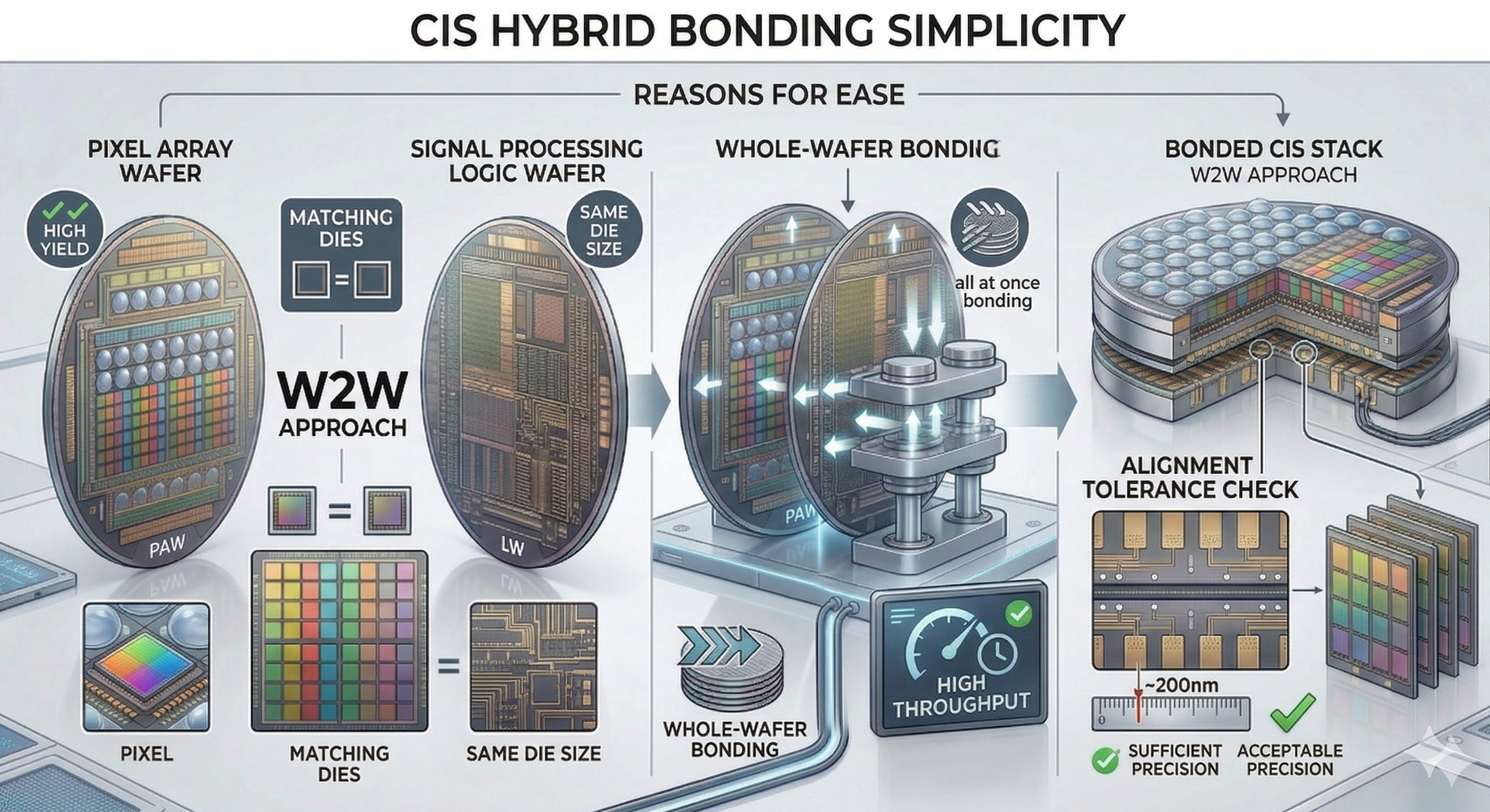
CIS was the first application to reach mass production with hybrid bonding. Sony’s IMX260, which shipped in the Samsung Galaxy S7 in 2016, was the first commercial product, built on Xperi’s (now Adeia) DBI (Direct Bond Interconnect) technology under license.
Hybrid bonding in CIS is relatively straightforward. The reason is simple: it uses wafer-to-wafer (W2W) bonding. The pixel array wafer and the signal processing logic wafer are bonded as complete wafers. Both wafers have matching chip sizes, and image sensors tend to have relatively high yields, making W2W viable. W2W bonds an entire wafer at once, which drives high throughput, and alignment precision of around 200nm is sufficient.
Key point: CIS is a two-layer stack. You bond two wafers. That’s it.
Logic/HPC (3D V-Cache, chiplets): the D2W domain
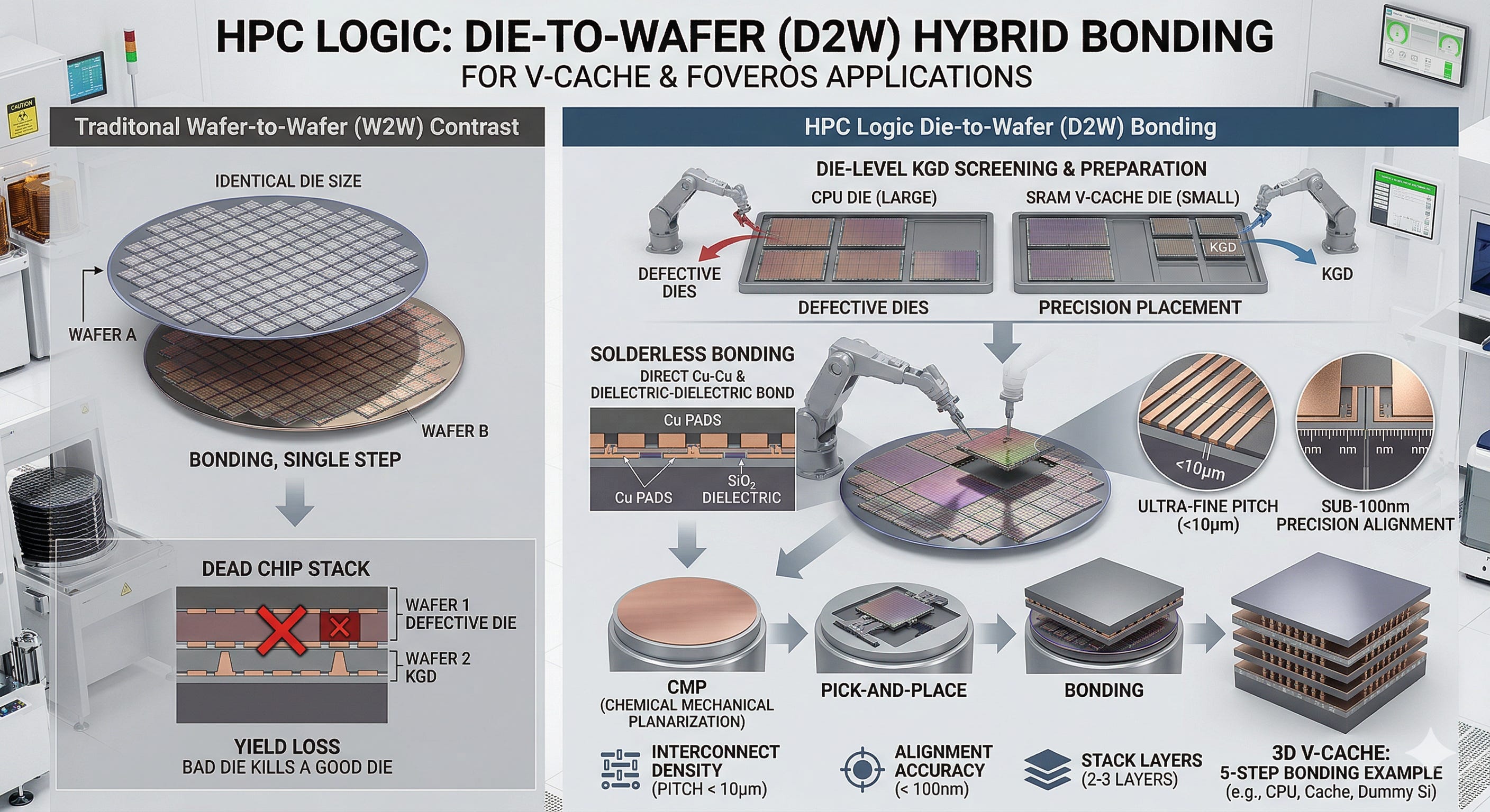
AMD’s 3D V-Cache is the defining example here. TSMC’s SoIC (System on Integrated Chip) platform is used to stack an SRAM cache die on top of a CPU die. Intel’s Foveros Direct falls in the same category.
These applications require die-to-wafer (D2W) bonding. Why not W2W? Because the two dies being bonded are different sizes.
The V-Cache die and the CPU die have different footprints. Combining chips of different dimensions requires placing individual dies onto a wafer one at a time.
D2W is technically much harder than W2W. Handling individual dies increases particulate contamination risk. The dicing process can introduce edge damage. Throughput is significantly lower than W2W.
The tradeoff is that D2W allows KGD (Known Good Die) selection, letting you screen out defective dies before bonding. With W2W, you bond entire wafers together, so a bad die on one side kills the good die it’s bonded to on the other.
Key point: Logic/HPC uses D2W, requires sub-10μm pitch, and demands alignment accuracy below 100nm. Typically two to three layers.