

The most expensive word in this AI cycle is bottleneck. As the datacenter bottleneck moved from compute to data movement, the memory companies holding HBM saw their stocks rerate first. As models grew, what ran short was not chip speed but the ability to feed data into chips.
The same logic carried straight over to optics. As light took over the distances copper could not cover, the entire optical value chain from transceivers to CPO got rerated. Memory and optics, the two protagonists of AI infrastructure investing, have been attacking the same bottleneck from opposite ends.
Yet the company standing where these two currents cross is surprisingly little known.
Avicena, an optical interconnect startup in Sunnyvale, California, counts Samsung Electronics, SK hynix, and Micron all on its cap table.
Three companies fighting each other for HBM share put money into the same private company side by side, and the light source this company uses to carry data is MicroLED.
Yes, the same MicroLED that was being built for displays.
This article covers why memory companies are paying attention to MicroLED, how this technology differs from conventional optical communications, what is moving on the ground right now, and what investors can take away from it.
Table of Contents
The Cap Table All Three Memory Makers Climbed Onto
LightBundle: Optical Communications Without the Laser
Where Wide and Slow Meets HBM
The Companies Following Avicena: Marvell, MediaTek, Credo, OSRAM
Comparing Against the Laser Camp: Where the Moat Is, and Where the Weaknesses Are
Investment Insight: Don’t Pick the Physics, Pick the Structure
Disclaimer
This article is for informational purposes only and is not a recommendation to buy or sell any security. Investment decisions and their consequences are the sole responsibility of the investor.
1. The Cap Table All Three Memory Makers Climbed Onto
To follow MicroLED optical communications, there is only one company you need to watch: Avicena. It is the clear leader in this technology, and it is no exaggeration to say that every company now trying to catch up is referencing its architecture.
Since its founding in 2019, it has held the title of the first company to use MicroLEDs for high-speed communications, and the research and products of later entrants take the structures it has published through conferences and papers as their starting point.
Start with the timeline.
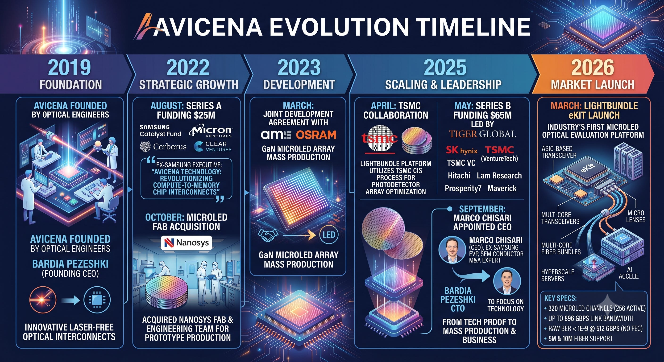
In 2019, engineers from the optical communications industry founded Avicena. Founder and first CEO Bardia Pezeshki built his career on laser-based optical communications. The person who knew lasers best started a company that threw the laser out.
August 2022: Series A of $25 million. Samsung Catalyst Fund, Micron Ventures, Cerberus Capital Management, and Clear Ventures participated.
The person who made the investment call on the Samsung side was Marco Chisari, then EVP at Samsung Electronics and head of the Samsung Semiconductor Innovation Center (SSIC). At the time, he commented that Avicena’s technology could be transformative in solving high-speed compute-to-memory chip-to-chip interconnect.
October 2022: acquired a MicroLED fab and engineering team from Nanosys, giving the company the means to produce its own prototypes.
March 2023: signed a joint development agreement with ams OSRAM for volume manufacturing of GaN MicroLED arrays.
April 2025: announced a collaboration with TSMC. LightBundle is the name of Avicena’s MicroLED interconnect platform, and the deal covers using TSMC’s CMOS image sensor (CIS) processes to optimize and mass-produce the photodetector arrays that go into it.
May 2025: Series B of $65 million. Tiger Global led, joined by SK hynix, Maverick Silicon, Prosperity7 Ventures (an Aramco affiliate), VentureTech Alliance (TSMC’s VC arm), Hitachi Ventures, and Lam Research.
September 2025: Marco Chisari joined Avicena as CEO.
The executive who had been running Samsung’s US foundry business and SSIC moved over to personally run the company he had invested in three years earlier. Pezeshki stepped into the CTO role to focus on technology development.
A semiconductor M&A specialist who handled the creation of GlobalFoundries and the acquisition of IBM Microelectronics took the CEO seat. The reasonable read is that the company has moved past the technology-proof stage and into the phase of production and deals.
March 2026: launched the LightBundle eKit, the industry’s first MicroLED optical communications evaluation platform, consisting of an ASIC-based transceiver integrating LED, photodetector, and microlens arrays plus a multicore fiber bundle.
Line up the investor roster in a single row: all three memory makers, TSMC’s VC arm plus a production partnership with TSMC itself, equipment maker Lam Research, and Middle Eastern sovereign wealth capital. Memory, foundry, equipment, and capital are all looking in the same direction.
The comment SK hynix left when it invested contains the exact problem this company is trying to solve.
High-speed electrical interconnects face a fundamental limit on reach, and laser-based optical links consume too much power.
MicroLED-based interconnects are therefore a promising low-power link candidate for the future memory fabric.
2. LightBundle: Optical Communications Without the Laser
Today’s datacenter optics are all laser-based. Whether transceiver or CPO, a DFB laser, an EML, or a VCSEL generates the light and a modulator loads the data onto it. The whole field has evolved in the direction of cramming as much data as possible onto the light from a single source: pushing serial rates to 100G and 200G per channel, using PAM4 modulation, bundling multiple wavelengths with WDM.
Avicena went in the exact opposite direction.
Instead of raising per-channel speed, it lowered it and multiplied the channel count into the hundreds. The company’s own phrase for this is “Wide and Slow.”
The structure works like this. On the transmit side, hundreds of blue GaN MicroLEDs are packed into an array. Each LED carries one independent data lane. The array couples into an imaging-grade multicore fiber bundle, and on the receive side, a matching array of silicon photodetectors (PDs) picks it up.
To borrow IEEE Spectrum’s framing, the transmitter behaves like a tiny display and the receiver behaves like a camera. With 300 pixels running at 10Gbps per lane, a single link can carry 3Tbps over more than 10 meters.
This architecture produces four points of differentiation.
First, there is no laser.
In laser-based optical links, most reliability, manufacturing, and cost problems trace back to the laser and to laser-fiber alignment. The reason CPO designs pull the external laser source (ELS) out into a replaceable module is that the laser is the component that dies first.
LEDs are structurally simple and tolerate a wide operating temperature range. At OFC 2023, Avicena demonstrated an optical link operating at 235°C, a temperature impossible for lasers. It sidesteps, at the light source level, the thermal dilemma of CPO, where the light source has to sit right next to a hot ASIC package.
Second, the power is in a different order of magnitude.
A laser does not operate below its lasing threshold. Whether or not data is being sent, current above threshold must always flow. LEDs have no threshold, so drive current can be lowered as far as the receiver’s SNR allows.
At SC25 in November 2025, Avicena presented results driving 4Gbps per lane at 100µA per LED while closing raw BER at 1E-12 without FEC. In transmit energy terms, that is 80fJ/bit. The company has also demonstrated sub-pJ/bit at the full link level, a full order of magnitude below the several pJ/bit range where laser-based optical interconnects are competing.
Third, it removes the SerDes.
Data inside a chip natively moves on wide parallel buses at around 2Gbps per lane. To send it off-chip, it has to be serialized into 100G-class signals and deserialized on the other end. That serialization and deserialization burns power, latency, and die area.
LightBundle takes the chip’s internal parallel data and maps it nearly 1:1 onto optical lanes. Modulation is plain NRZ, not PAM4. No DSP is needed, and since no FEC is needed, there is no FEC decoding latency either.
Fourth, very few components need to be invented.
MicroLED arrays are something the display industry already mass-produces, and silicon PD arrays are something the CIS industry already mass-produces, both at the scale of hundreds of millions of pixels. LEDoS for AR glasses integrates LEDs at micron-scale pitch, and smartphone CIS chips stamp out pixels by the hundreds of millions. Next to that, the channel count Avicena needs is in the hundreds.
Unlike silicon photonics, which has to mature new components like ring resonators and comb lasers, this approach can be built as a variation on existing industrial ecosystems.
TSMC bringing its existing CIS process portfolio directly to PD array production is the proof point.
The “leverage the existing ecosystem” logic comes with a caveat. MicroLEDs for communications have different requirements than MicroLEDs for displays. Displays care about brightness and color; communications care about modulation bandwidth. LED devices that can switch at GHz rates have to be developed separately, individual devices must shrink as integration density rises, and bonding yield on CMOS at tight pitch has to be secured.
The soil of the ecosystem can be borrowed, but the crop has to be grown fresh.
According to current employees at SK hynix, Samsung, and Micron in my industry network, all three memory makers are now very seriously evaluating MicroLED for memory optical interconnect. That is what prompted this article.
Below, I will walk through, one by one and in detail:
Why it is the three memory makers, of all companies, that are carefully evaluating this technology right now
How MicroLED and HBM lock together at the level of design philosophy
What is happening on the ground in a field that Marvell and Microsoft have now entered
And where the investment insights that others have not yet found are hiding.