Memory-on-Logic: Re-Rating Memory Beyond the Cycle

The market and a number of recent reports have grown bearish on memory. The thesis runs that the wave of capacity additions arriving around 2027 and 2028 will let supply catch up with demand, prices will roll over, and a de-rating will follow just as the old cyclical script dictates.
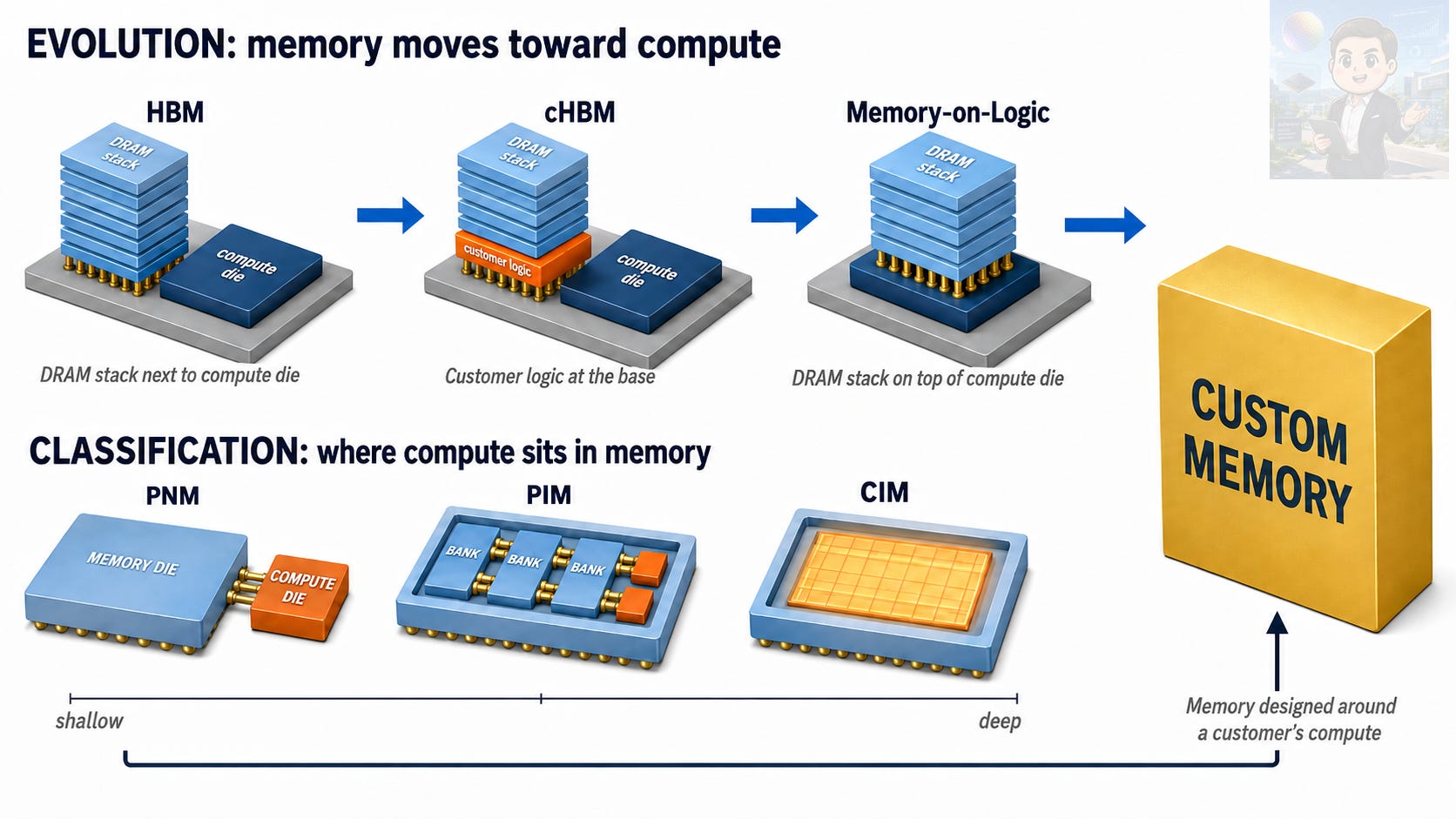
The last piece followed the structural evolution from HBM to cHBM to memory-on-logic, using HBM as the reference application, and argued that the memory business is turning into a custom silicon business.
This piece takes a more general, functional angle. The idea is to classify custom memory by function, by what memory does beyond storing data. The industry uses three names for this axis, CIM, PIM, and PNM. The boundaries between these terms vary from company to company and paper to paper, and some use PIM as an umbrella for every compute-in-or-near-memory structure. To avoid confusion, this piece draws the lines by the physical location of the compute.
CIM (Compute-In-Memory) uses the electrical behavior of the memory cells or the array itself to perform computation. It exists in both analog and digital forms, and it is the deepest that compute can go.
PIM (Processing-In-Memory) keeps the cells as storage and places compute units inside the same DRAM die, next to the banks or in the peripheral circuitry.
PNM (Processing-Near-Memory) moves the compute onto a separate logic die outside the memory die, connected to the memory through a very wide, very short path. It is the shallowest of the three, and Qualcomm’s recently announced HBC is exactly this structure.
My thesis has been the same since the last piece.
The memory business is turning into a custom silicon business, and commodity memory that anyone could buy is evolving into custom memory designed for specific customers. The last piece traced that transition along the position axis, where the memory sits. The three names in this piece trace the same transition along the function axis.
Memory is moving toward compute, and compute is walking into memory, two flows in opposite directions converging on the same place. With two axes, a single product can hold one coordinate on each, so a product from the last piece appearing again here does not mean its classification changed.
This piece unpacks the technology so that readers without a hardware background can follow it comfortably. It closes with my own view, worked out in numbers, on how much this transition dampens the next cycle that could follow the record capacity buildout. Anyone with money in memory should read through to the end.
Contents
Why Compute and Memory Live Apart
The Balance AI Broke
The Price of Custom Memory, and Why It Is Back on the Table
Two Answers, PIM and PNM
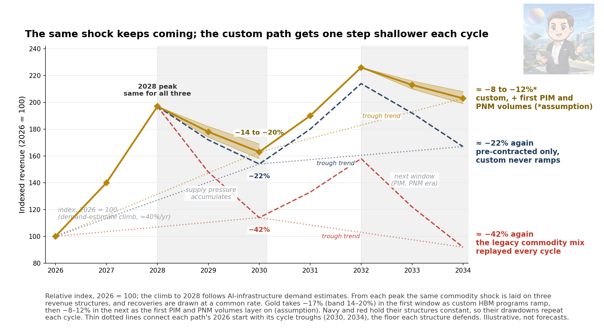
My View, How Much Custom Memory Dampens the Next Cycle
Disclaimer
The figures and facts cited in this piece are drawn from public sources. The interpretations and scenarios are entirely my own analysis. Nothing here is a recommendation to buy or sell any security, and investment decisions and their consequences rest with the investor.
1. Why Compute and Memory Live Apart
Every computing system splits into two parts, a processor that does the work and memory that holds the data. Keeping compute and storage apart and wiring a path between them is the basic skeleton of nearly every computer we use.
It is called the von Neumann architecture.
Watch a processor do a single addition. The structure of A+B=C lives on the processor, while the values A and B live in memory. The processor fetches 2 and 1 from memory, adds them, and writes the result 3 back. Compute on the processor, data in memory, signals shuttling between them without pause. That is the basic motion of computing.
On physics alone, the best structure is obvious. Put the processor and the memory as close together as possible. Shorter signal paths mean lower latency and lower energy at the same time, so integrating both on one die wins on performance and on power.
Such a memory exists. It is SRAM, the memory that sits on the processor die and answers within nanoseconds, the one we know as cache. Its problem is density. Each cell burns six transistors, so growing the capacity would let the memory eat the processor’s die. SRAM stays a small vessel for only the hottest data.
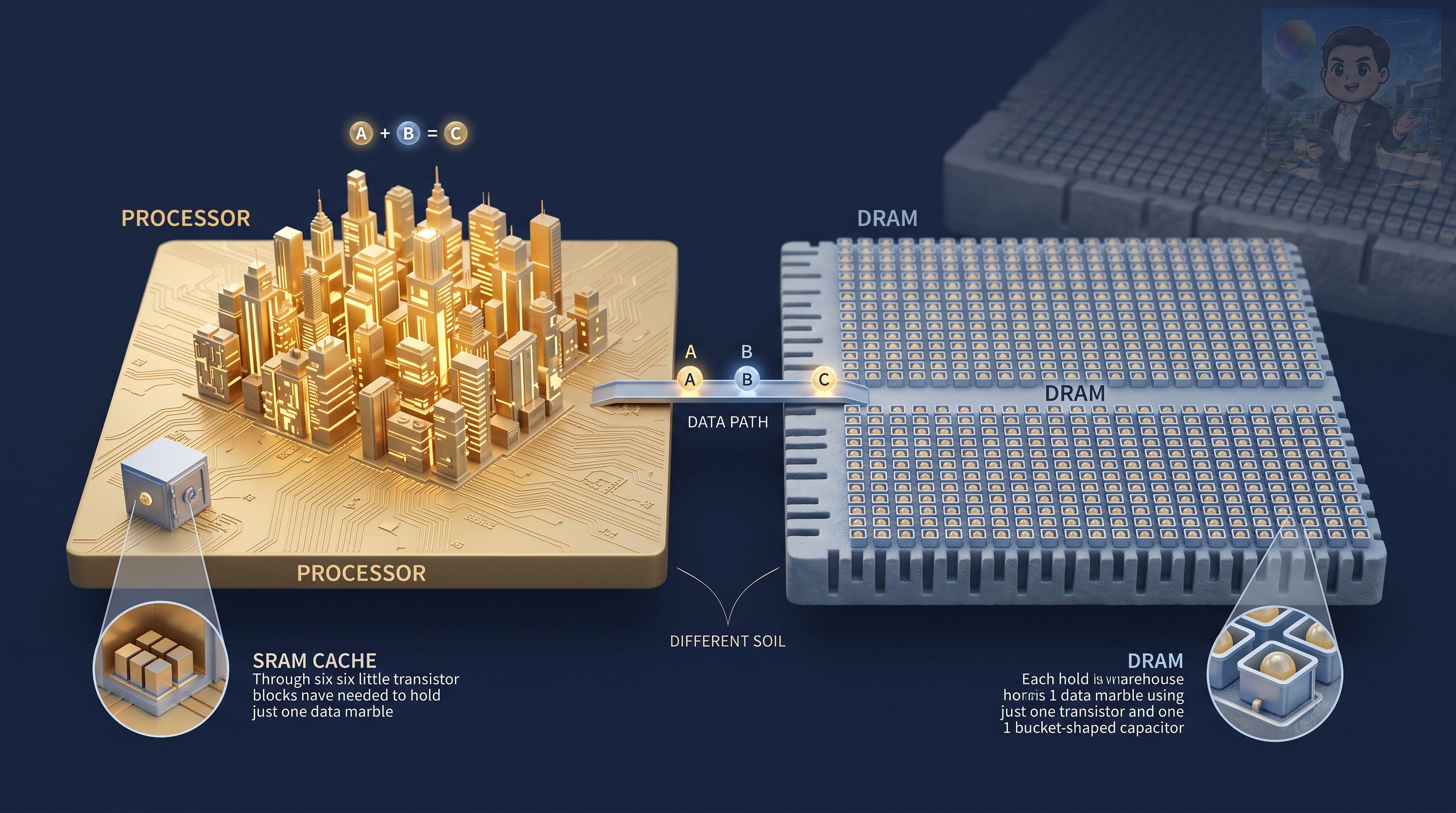
DRAM is the answer from the other side. One transistor and one capacitor per cell packs far more data into the same area, but it cannot ride on the same die as the processor.
The reason sits in the process technology. A DRAM process is tuned entirely around building capacitors densely and keeping them from leaking. Draw logic circuits on that ground and the same circuit comes out larger and slower than it would on a logic process. Building DRAM cells on a leading-edge logic process fails the other way, on cost. Ground that suits logic and ground that suits memory are different ground. Economically integrating high-density commodity DRAM with cutting-edge logic on one die has never worked.
So the industry chose separation. Processor die here, DRAM die there, wired together across the board. Out of that choice came the memory hierarchy we know, near and small SRAM, far and large DRAM, farther and larger storage. The split von Neumann drew on paper was carved into silicon as a die boundary.
The road memory technology has walked since then fits in one sentence. Get close again, somehow. Interface speeds rose generation after generation. GDDR widened the pipe beside graphics chips. HBM took the seat right next to the GPU on a shared silicon substrate, the interposer. Memory-on-logic, covered in the last piece, puts memory directly on top of the processor, the physical end of this road.
This history of closing the distance shares one trait.
What moved was always the data or the memory. Caching copies hot data next to the processor. HBM and memory-on-logic pull the memory die itself toward the processor. Moving the compute has never been the industry’s mainstream answer. Which leaves one idea on the table.
Do not move the data. Move the compute.
This is where the names CIM, PIM, and PNM were born. Carve off part of the compute logic and send it across the boundary. The moment you send it, a question follows. How far, and into which die. To see why this idea got serious now of all times, start with what AI began demanding from memory.
2. The Balance AI Broke
The shuttling between processor and memory was not a problem for a long time. Once the processor fetched data, it had plenty to do with it. As long as compute was heavy and data was light, the cost of the round trip hid behind the compute time.
AI inference flipped that ratio.
Each time an LLM produces one output token, it must read the entire set of model weights from memory once. It pulls in hundreds of gigabytes, and the work it does with them is multiplication and addition. Measured in operations per byte, the workload is punishingly light, so the processor spends much of its time waiting for data to arrive. GPU compute jumps several fold each generation while memory bandwidth does not, and the gap keeps widening.
This is why HBM commands its price, and why memory became the accepted bottleneck. No matter how fast the processor gets, a narrow data path wastes it.
The wall has an old name, the von Neumann bottleneck.
The industry’s first response was more of the same closing of distance. Closer, wider. HBM has widened its interface and stacked higher with each generation. But there is a question that comes at the problem from a different angle.
Can the amount of data sent be reduced at the source?
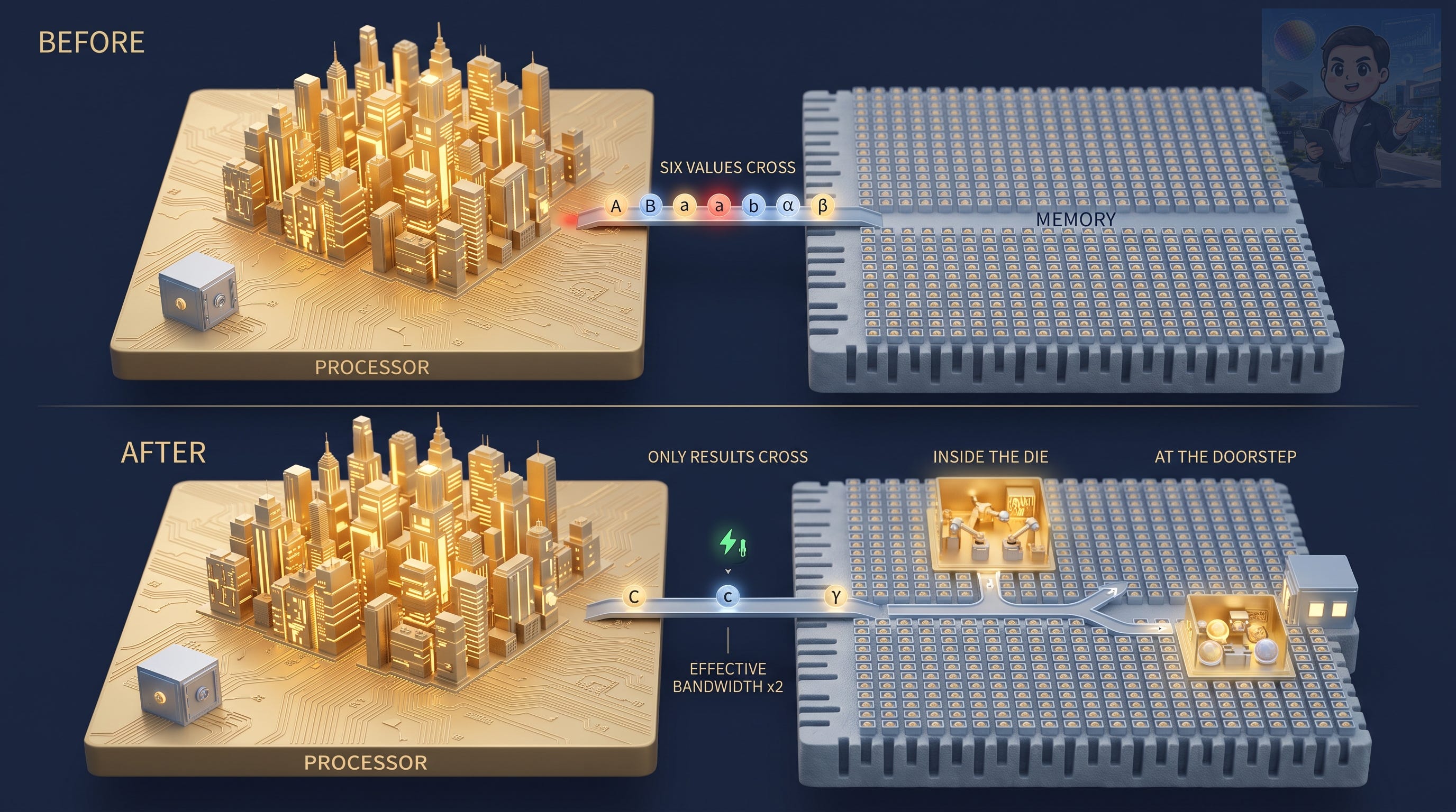
Return to the addition example. If the processor must compute (A+B), (a+b), and (α+β), the existing structure moves six values, A, B, a, b, α, and β, from memory to the processor. If the memory knows how to add, only three values need to cross, C, c, and γ. Not one wire was added and not one pin ran faster, yet the data crossing the boundary halved. The effect equals doubling the usable bandwidth. Fewer bytes moved also means less power spent moving them.
In today’s systems, moving data costs far more energy than computing on it, so this is a power story as much as a performance story.
The example also previews a fork in the road. The idea of taking compute to the data is shared, but how far you take it splits the path in two. Bring it inside the memory die, as CIM and PIM do, and the volume of data sent shrinks at the source, but touching the inside of the memory makes this a road only memory makers can walk.
Take it only to the memory’s doorstep, as PNM does, and the raw data still crosses to the adjacent logic die, but only results travel on to the host, easing the outer path. Since nothing inside the memory changes, companies that buy memory can walk this road too. In silicon terms the fork reduces to one sentence. Put the compute inside the memory die, or attach it beside the memory as a separate die.
Compute where the data lives, and send only the results. That single line is the skeleton of CIM, PIM, and PNM alike. If the bottleneck is movement, reduce the movement. It sounds more obvious the longer you listen. Yet this obvious idea sat in papers for decades and is still climbing over the threshold into commercial products. Not because the technology fails, but because of the price tag attached to the idea.
From here, the piece walks through why this good idea went uncommercialized for decades, how it is becoming product in the field right now, and my view on how much this transition dampens the next cycle.
3. The Price of Custom Memory, and Why It Is Back on the Table
Standard memory’s strength lies in a fully standardized interface.
A DRAM die operates only on commands agreed at JEDEC, the standards body that sets the memory industry’s common specifications. Give it an address and it returns a value. Give it a value and it stores it. Whether the chip above it is an Intel CPU, an NVIDIA GPU, or some startup’s accelerator, the behavior is identical. That is what made same-spec memory from Samsung, SK hynix, or Micron interchangeable commodity. Memory prices riding the spot market, and customers holding the bargaining power, both flow from that interchangeability.
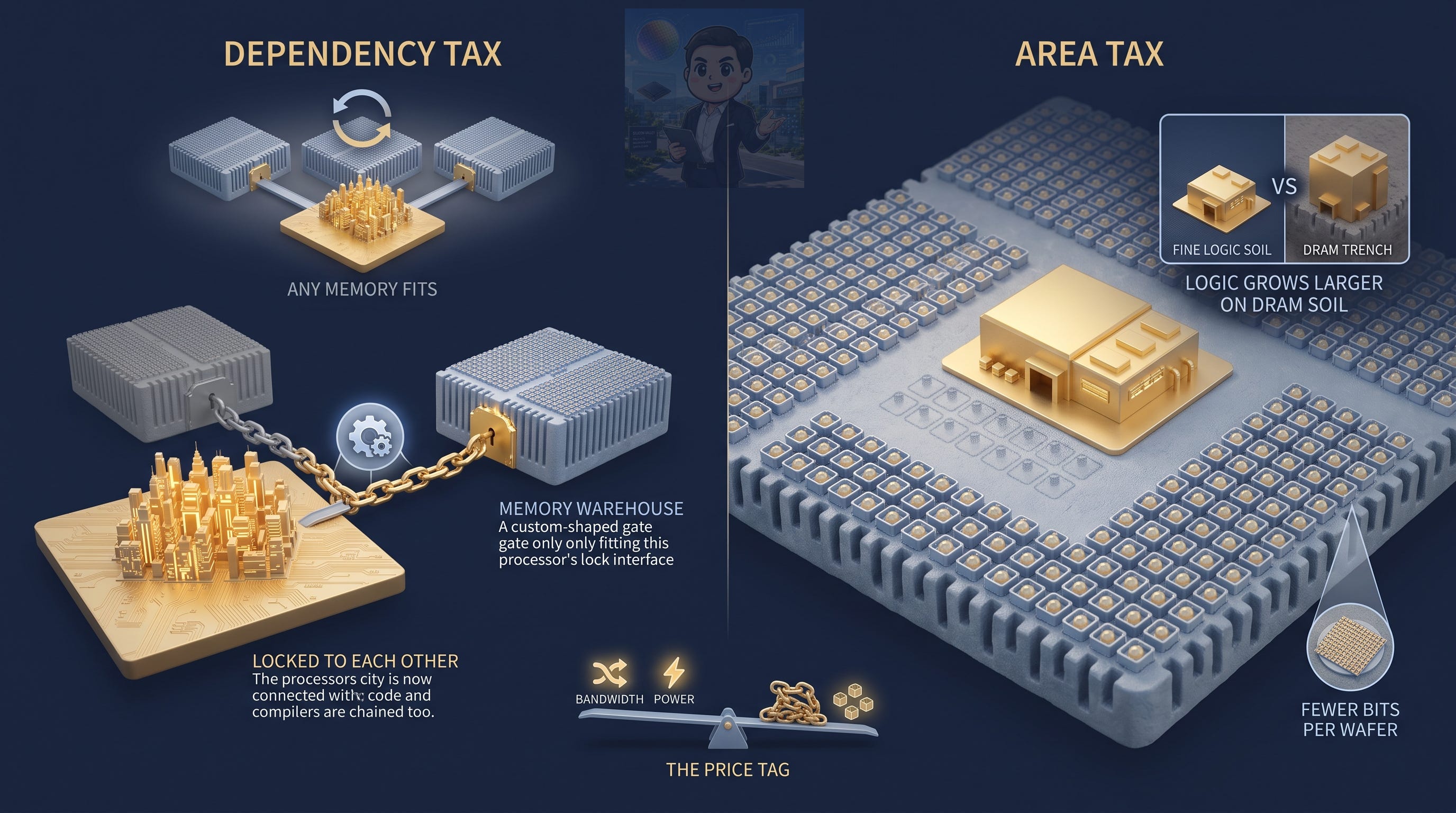
Put compute into the memory and the interchangeability breaks. Suppose the memory learns to add. It must now understand a command that does not exist in the standard, fetch the result of the addition. The processor must be designed around that command. The software must know where the boundary sits and split the code, deciding which operations go to the memory. Memory and processor become locked into each other’s designs. That is the first tax, the dependency tax.
There is a second tax, the area tax. Compute logic occupies ground where cells would have stood. Worse, a DRAM process is barren soil for logic, so the same compute circuit draws larger there than it would on a logic process and takes even more room. Recall that a memory maker’s profit formula starts with how many bits come off one wafer, and the weight of this loss becomes visible. A company whose core business is packing more bits into the same area is planting compute where bits would grow. The density loss is a cost-structure problem before it is a spec-sheet problem.
To sum up, putting compute into memory buys bandwidth and power at the price of two taxes, dependency and area. That is why a technology researched for decades never reached commercial products.
So why is it back on the table now?
Because the math of gains against taxes has changed.
On the gains side, AI inference pushed memory bandwidth to the top of the bottleneck list, making the value of reduced data movement larger than it has ever been.
On the tax side, the base die’s move to logic processes created a place for compute to land, and the dependency that remains can be passed through to price.
Memory tailored to a specific customer bills a premium and development fees rather than the commodity spot rate. A business that rode the spot market can become a business that holds contracts. That is why this story about taxes is ultimately a story about margins.
4. Two Answers, PIM and PNM
Of the three answers, the deepest, CIM, uses the electrical behavior of the cells or the array itself for computation. Research continues in both analog and digital forms, but its taxes are the heaviest and no product carries a commercial schedule, so it ranks low on this piece’s investment clock.
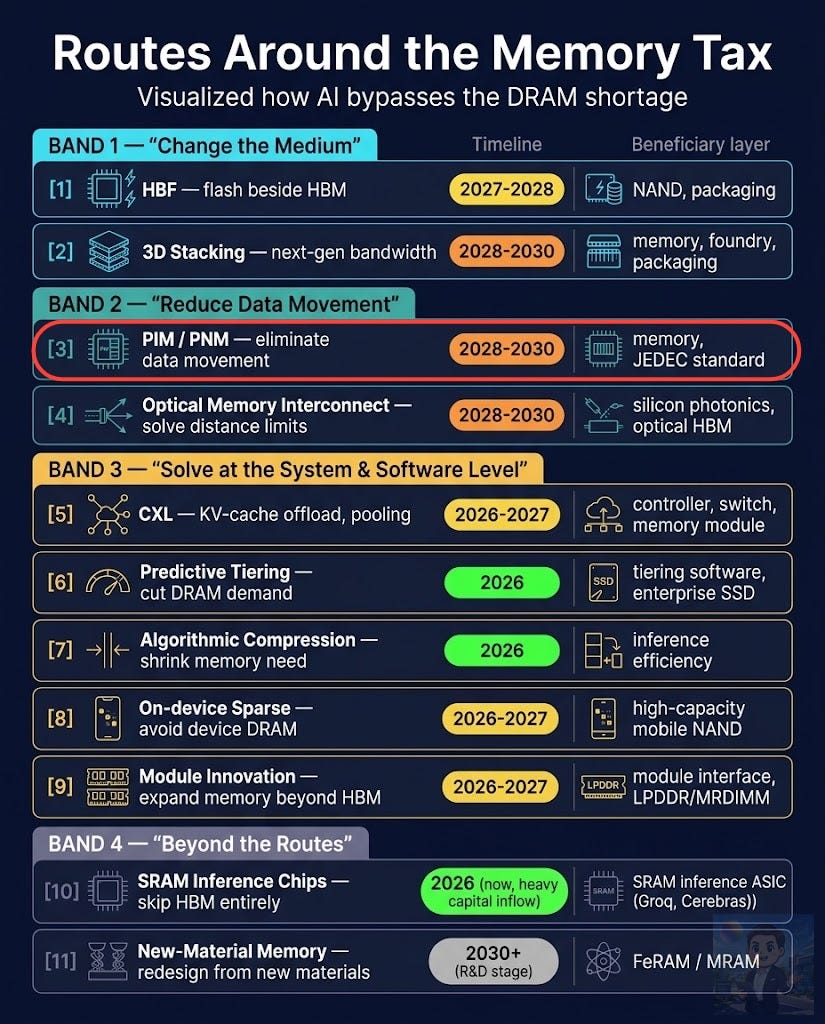
The two that have crossed into actual products are PIM and PNM. Last month’s piece mapping nine branches of solutions to the memory bottleneck introduced these two as one branch, and that branch already has concrete products and companies standing on it.