

On June 30, 2026, Etched came out of stealth after more than two years of silence. The company reported a successful first silicon tapeout (A0) on TSMC’s N4P process, over a billion dollars in customer contracts, $800 million in cumulative funding, and first racks shipping this summer. A company that had said nothing for more than 20 months had moved to working silicon and rack-level product validation.
Announcements like this now arrive every quarter. In December 2025, Nvidia licensed Groq’s inference technology in a deal reported at roughly $20 billion and brought over its key people. In May 2026, Cerebras went public and touched nearly $80 billion in intraday market cap on its first day. In June, reports followed that Qualcomm was in talks to acquire Tenstorrent at $8 to $10 billion.
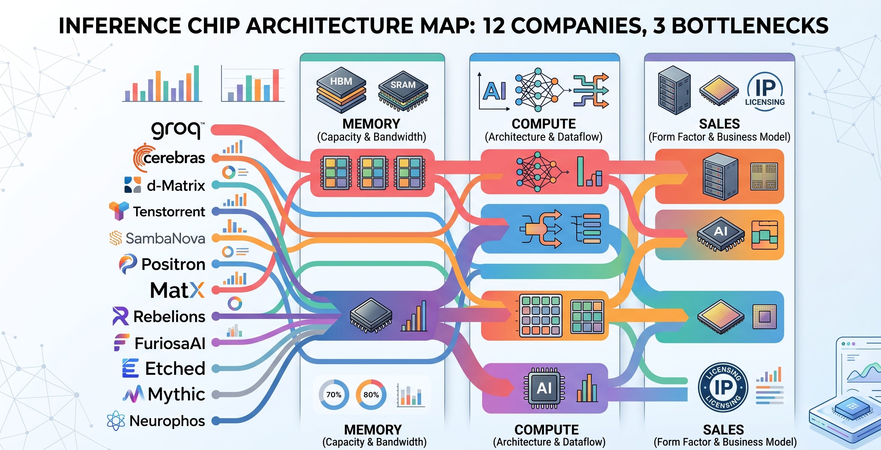
Behind this run of inference chip companies getting acquired and listed is a bet by capital markets that the spread of AI agents will drive a surge in inference demand. But this is not a race you can rank on speed alone. Even among inference chips, the character of the business changes completely depending on where you put the memory, how much you fix the compute, and whether you sell a chip or a system. Each of those choices targets a different workload that Nvidia does not cover efficiently.
So reading these companies properly means looking at the technical choices each one made before looking at valuation or speed. Layer the map of the startups on top of how Nvidia and the hyperscalers defend and encroach on the same market, and the actual size of the space these companies can capture comes into view.
This piece starts by splitting the problem of inference into three bottlenecks. It lays out how the 12 companies answered each bottleneck using measured specs, then goes deep by memory camp to show how each choice actually works in practice. After that it looks at how Nvidia and the hyperscalers press this market from above and below, and where the real space for startups sits in between. The aim is a picture of where the whole contest is heading, rather than which individual company wins.
Table of Contents
Inference has three bottlenecks
How 12 companies answered the bottlenecks
A deep dive into four camps
How Nvidia and the hyperscalers respond
Disclaimer
This piece is an analysis based on public materials and company announcements, and does not recommend buying or selling any security. Valuations and technical claims for private companies rely mostly on the companies’ own disclosures and are often hard to verify independently. The acquisition material includes negotiations that have not yet closed. Chip specs are based on each company’s public materials and can vary by generation and configuration. Responsibility for any investment decision rests entirely with the reader.
1. Inference has three bottlenecks
Training and inference are the same AI, but the character of the computing is entirely different. Training is a one-time job that teaches a model on massive data. Inference is the standing job of running the trained model to generate tokens.
Most of the headlines went to training, but the side that drives real cost is inference. Every query and every agent call burns power and cycles every day. As coding agents and autonomous agents proliferated through the second half of 2025, that burden grew exponentially. An agent breaks a task into multiple steps, calls the model in a chain, and at each step generates tokens that feed back in as input.
For an inference chip to differentiate from a GPU, it has to solve the problems a GPU runs into during inference. Those problems break into three bottlenecks.
Bottleneck 1: memory bandwidth. The token generation step of inference, the decode phase, reads the entire set of model weights back from memory every time it produces a single token. Generating 10 tokens per second means reading several terabytes of weights per second for a single user. During this, the compute units sit mostly idle, and the speed of pulling data from memory determines overall performance. No matter how high the FLOPS, they do not help if memory bandwidth is low. This is the memory wall, and it is the most fundamental constraint in inference chip design.

Bottleneck 2: the cost of flexibility. A GPU is designed to handle general-purpose compute. The price of that generality is that transformer inference spends cycles on instruction fetch, thread scheduling, and kernel launch overhead, which pushes utilization far below peak performance on many inference workloads. The more you fix the hardware to a specific workload, the more you cut this waste, but the more you fix it, the less you can run other models. Flexibility and efficiency are in tension.
Bottleneck 3: deployment and power. However fast a chip is, you cannot sell it if you cannot fit it into a data center rack and handle the power and heat. Large models in particular need more than one chip, so you have to tie several together, and at that point the interconnect between chips, the cooling, and whether you can deploy into a standard data center within days decide the outcome in the field.

The three bottlenecks are not independent. They connect in sequence. Which memory you pick in Bottleneck 1 constrains Bottleneck 2, meaning which models you can run and how flexibly. SRAM alone is fast but cannot hold large models. Adding HBM raises capacity but carries supply and packaging burdens.
The memory and compute structure set by those choices then governs the system design of Bottleneck 3, meaning how many chips you tie together and in what form you sell them. Viewed along these three axes, the 12 companies reveal not a roster of names but a map of design philosophies.
2. How 12 companies answered the bottlenecks
The table below lays out how each company answered the three bottlenecks, using measured specs. The status column marks licensed, listed, in acquisition talks, or private, separating those that have already exited or been absorbed into a large company from those still independently private.
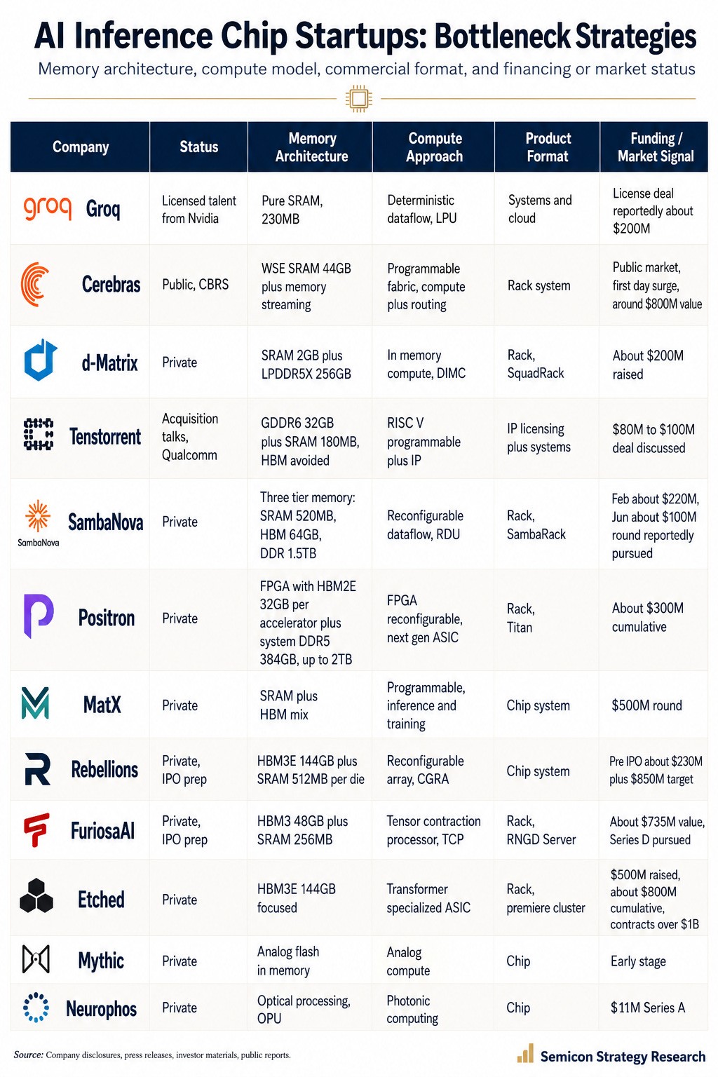
What matters in this table is not the company names but the fact that the inference chip market is not one market. Some companies try to avoid HBM. Some grip HBM harder. Some pull the memory bottleneck inside the chip with SRAM. Some change the cost structure with DDR and LPDDR.
So this contest is less a question of who is faster than Nvidia and more a question of who solves, more cheaply, the bottleneck Nvidia is solving expensively. Read each column of the table through that lens and the map of design philosophies appears.
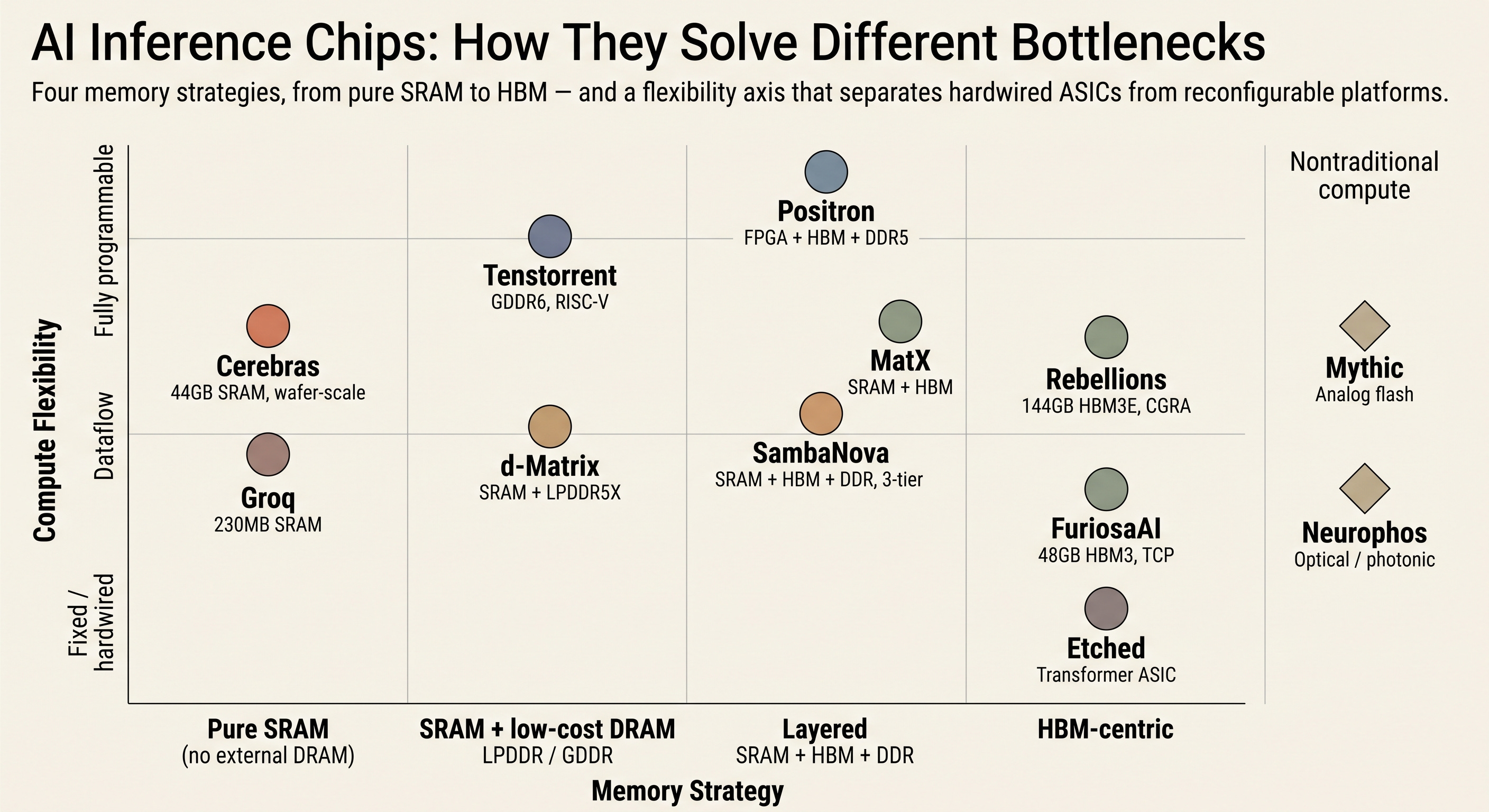
Run down the Bottleneck 1 column from top to bottom and the fundamental structure of the inference chip market comes into view. Only two designs minimize HBM dependence with an SRAM-centric approach. Groq and Cerebras share that SRAM-centric philosophy but go about it differently.
Groq cuts latency with deterministic dataflow on 230MB of on-chip SRAM. Cerebras pairs the WSE’s 44GB of SRAM with MemoryX-based weight streaming to handle large models. With a 190x gap in on-chip capacity, the strategies split. Groq’s SRAM is small, so running a large model requires a system design that ties many chips together, while Cerebras puts a large model onto a single wafer.
The second group uses SRAM but reinforces capacity with low-cost DRAM instead of HBM. d-Matrix attaches 256GB of commodity LPDDR5X to 2GB of on-chip SRAM, and Tenstorrent uses GDDR6. Both deliberately sidestep HBM’s supply crunch, price, and packaging complexity. Tenstorrent CTO Jim Keller has said publicly that you cannot beat Nvidia as long as you use HBM.
The third group folds HBM into a tiered structure. SambaNova stacks SRAM, HBM, and DDR across three tiers, keeping multiple models in memory and swapping them in milliseconds. Positron attaches DDR5 to an FPGA that already carries HBM.
The fourth group puts HBM at the center. Rebellions secures capacity with 144GB and FuriosaAI with 48GB of HBM. There is a contrast worth noting. Rebellions carries 512MB of on-chip SRAM per die, more than FuriosaAI’s 256MB. Even within an HBM-centric approach, on-chip memory strategy differs by company.
Look at the Bottleneck 2 column and a spectrum of flexibility appears. At one end sits Etched, a specialized ASIC that etched transformer operations into silicon. That said, in the June 30 announcement Etched stated that customers are validating it beyond the transformer-only design it was originally known for, extending to DeepSeek, Qwen, Mamba, and Llama. The inclusion of Mamba, an SSM, and DeepSeek, an MoE, signals support for a wider range of models than the pure hardwired framing suggested at first.
At the other end sits Positron. An FPGA physically reconfigures its gates, so it carries the highest flexibility. In between sit reconfigurable arrays (Rebellions’ CGRA), reconfigurable dataflow (SambaNova’s RDU), deterministic dataflow (Groq’s LPU), and tensor contraction processing (FuriosaAI’s TCP).
What stands out in the Bottleneck 3 column is that almost every company converges on a rack-level system. As customers want deployable infrastructure rather than a single slice of silicon, selling chips alone has become a hard way to win the market. That is why the large rounds cluster around the companies selling systems. The outlier is Tenstorrent, which licenses the design as IP rather than selling chips, letting customers own their own silicon.
3. A deep dive into four camps
If the table above is a snapshot showing each company’s choice at a glance, this section looks at how those choices actually work in practice. The order follows the four memory camps of Bottleneck 1. For each camp it traces how far the representative company has come, then sets out what the camp means for the market.
That meaning does not stop at memory. Within each camp, Bottleneck 2, meaning how flexible the compute is, is set in lockstep with the memory choice, so each camp’s memory strategy and flexibility position are read together.
The SRAM-centric camp: Cerebras and Groq
Cerebras WSE-3: The Technical Achievement and the Physical Ceiling

Cerebras Systems’ WSE-3 hit 2,522 tokens/s per user on Llama 4 Maverick inference. That is more than double the 1,038 tokens/s NVIDIA published for the DGX B200 on the same model.
Cerebras solves the problem with wafer-scale integration. An ordinary chip is cut from a 300mm wafer into hundreds of pieces, but Cerebras does not cut the wafer and uses the whole thing as a single chip. So the WSE-3 holds 44GB of SRAM on a single chip, and that SRAM sits right next to the cores, delivering 21 petabytes per second of bandwidth.
For large models that do not fit entirely in on-chip SRAM, it uses weight streaming, flowing weights in real time from an external memory device called MemoryX. The strength is that it can run large models without splitting them across chips, and without attaching HBM to the WSE itself.
The financials that surfaced after listing show both sides of this technology. Revenue in 2025 was $510 million, up 76%, but 86% of it came from two affiliated entities in the UAE. The technical moat of wafer-scale is deep enough to be nearly impossible to copy, but the stability of the business is still tied to customers in a single region, and the pace at which the OpenAI and AWS contracts convert from on-paper backlog into actually recognized revenue is the thing to watch.
Groq’s LPU solves the same problem a different way. On-chip SRAM is 230MB, one 190th of Cerebras’, but in exchange it chose deterministic dataflow that fixes the order and timing of every operation at the compile stage. There is no scheduling waste during execution, so token generation latency is extremely short. The trade-off is that the small SRAM means running large models requires a system design that ties many chips together.
In December 2025, Nvidia secured a non-exclusive license to Groq’s inference technology and brought over key people including founder Jonathan Ross. The deal was reported at roughly $20 billion, but it is a license rather than an acquisition, and Groq itself remains an independent company with Simon Edwards as its new CEO, continuing to operate GroqCloud. Groq’s latency optimization is now an element used even inside Nvidia’s own inference stack.
The reference points these two companies gave the market are twofold.
One is a valuation benchmark. Groq priced in at roughly $20 billion through a license deal, and Cerebras at nearly $80 billion in intraday market cap on its first day of trading, which became the yardstick for valuing the rest of the still-private companies.
The other is more fundamental. An SRAM-centric bet means growing on-chip memory to the limit, and that SRAM is not a separate component but silicon printed on the wafer inside a logic fab. The more SRAM-centric design and in-memory compute grow, the more that volume flows to foundry silicon area rather than the DRAM of the three memory makers. If this trend grows, part of memory demand shifts from DRAM to the foundry.
On flexibility, this camp is the side that has largely given it up. Groq’s deterministic dataflow fixes execution order at compile time to cut latency, giving back runtime freedom in return. Cerebras keeps programmability, but the constraint of fitting a whole model onto a single wafer limits flexibility in its place. The choice to pull memory inside the chip leads directly to a choice that fixes compute to a specific execution style. The principle that memory choice sets the degree of freedom in compute shows up most clearly in this camp.
The low-cost DRAM camp: d-Matrix and Tenstorrent
d-Matrix competes with DIMC, digital in-memory compute. An ordinary chip pulls data out of memory and moves it to compute units to calculate, but DIMC embeds multipliers inside the SRAM circuit so the compute happens right where the data is stored, eliminating data movement itself. Where analog in-memory failed to commercialize because of accuracy loss, d-Matrix held enterprise-grade precision with a digital approach.
It attaches 256GB of commodity LPDDR5X to 2GB of on-chip SRAM to secure large capacity without HBM. By placing this chiplet on an organic substrate instead of the CoWoS used for HBM, it avoids both the chronic HBM supply crunch and the fight for CoWoS capacity at once. In June 2026 the flagship Corsair entered mass production, roughly 90% of customers are in the US, and it has secured commitments from hyperscalers and frontier labs.
Tenstorrent, led by Jim Keller, has a clear strategy. On the judgment that you cannot beat Nvidia as long as you use HBM, it uses standard GDDR6. Its compute unit, the Tensix core, bundles matrix and vector units with multiple RISC-V cores, and being based on an open-source instruction set, it carries high flexibility.
The differentiator is that it does not just sell chips but licenses this design as IP, securing roughly $150 million in IP contracts with Samsung, Hyundai, and LG. In April 2026 it shipped Galaxy Blackhole, and in June came reports that Qualcomm was pursuing an acquisition at $8 to $10 billion. That said, this deal is closer to buying IP and talent than chips, so the question of what remains if Keller leaves after the contract period follows it.
What these two companies target is the packaging bottleneck. Using HBM requires the advanced packaging called CoWoS, and Nvidia takes most of that capacity, so for new entrants supply is as much of a problem as performance. d-Matrix choosing an organic substrate and Tenstorrent choosing GDDR are attempts to route around this bottleneck. The more their approach proves valid, the more a portion of the inference chip market flows down a path that does not pass through HBM and CoWoS. This is the camp that cracks the assumption that HBM demand grows one-to-one with the spread of inference.
If CoPoS Arrives, Who Makes Money First

In AI chips, packaging has become the process that decides performance. As chip miniaturization hits its limits, the method of binding several chips into one has grown more important, and the standard for that is TSMC's CoWoS. TSMC is now preparing CoPoS as the next step beyond CoWoS. Instead of a round wafer, it places chips on a square panel.
On compute flexibility, this camp stands at the opposite pole from the SRAM-centric camp. Having solved the capacity constraint with low-cost DRAM, there is no reason to bind compute to a specific execution style, so flexibility is left wide open. Tenstorrent’s Tensix core being open-source RISC-V based, and its design licensed as IP so customers can put it on their own silicon, is the extreme of that. The room secured by avoiding HBM comes back as freedom in compute.
The tiered camp: SambaNova and Positron
SambaNova chose a three-tier memory structure. It stacks 520MB of on-chip SRAM, 64GB of in-package HBM, and 1.5TB of external DDR as tiers, keeping frequently used weights in SRAM, the current model in HBM, and models waiting to be swapped in DDR. This structure of loading multiple models and swapping them in milliseconds fits the pattern of agents that switch models often.
Its valuation trajectory shows the company’s ups and downs. It peaked at $5.1 billion in 2021 and came down, Intel’s $1.6 billion acquisition offer fell through at the end of 2025, and the implied valuation of its Series E in February 2026 was around $2.2 billion. Then in June came reports that it was pursuing a new round at a $10 billion valuation. It shows the overheating of the inference market lifting even the value of a company that had been going through down rounds.
Lip-Bu Tan has served as SambaNova’s chairman since 2024 while also serving as Intel’s CEO, which makes it a company with deep capital and governance ties to Intel as well.
Positron made a choice others did not. It built its first-generation Atlas out of an FPGA rather than a custom ASIC. An FPGA is less efficient than a dedicated chip but greatly shortens the time from design to shipment. Positron deliberately took this trade-off and shipped product within 15 months of founding, with 15 people and under $12 million. It put physical hardware into data centers at a point when competitors had not yet finished their chips.
To this it added the supply chain advantage of full-process production in Arizona and the convenience of OpenAI API compatibility. The memory is a tiered structure of FPGA-embedded HBM with DDR5 attached. The next task is the transition to a custom chip, Asimov, targeting 2TB of memory per chip with a tapeout planned for the second half of 2026. Whether the advantage of entering first, bought with time by the FPGA, holds through the transition to Asimov, an entirely different piece of silicon, is the inflection point.
The tiered structure changes the shape of memory demand itself. Pure SRAM is fast but small, HBM is large but supply-constrained, so no single one suffices and you stack layers. SambaNova’s three tiers and Positron’s HBM-plus-DDR configuration are the same idea. This means that when one inference chip is added, memory sells not as one type but as several types at once. This structure carrying HBM and DDR5 together shows a different picture from the assumption that the spread of inference grows only HBM demand.
This camp’s flexibility comes not from the compute style but from the memory hierarchy. SambaNova’s structure of stacking multiple models in layers and swapping them in milliseconds secures, through memory placement rather than hardware, the flexibility of one chip moving across multiple workloads. This approach fits the pattern of agents chaining calls to different models at each step. The compromise of fixing compute while securing flexibility through memory is the real reason for stacking layers.
The HBM camp: Rebellions, FuriosaAI, Etched, MatX
Rebellions uses CGRA, coarse-grained reconfigurable array. It reconfigures the connections between neural cores in software, adjusting the data flow even while inference is running. While securing capacity with 144GB of HBM3E, it carries 512MB of on-chip SRAM per die, more than FuriosaAI in the same camp.
Its valuation jumped from $1.4 billion in September 2025 to $2.34 billion six months later, and it raised $650 million over the past six months. It is preparing an IPO, and with Samsung and SK Hynix participating as investors at the same time, it holds a structural advantage in securing HBM during a supply-crunch phase.
FuriosaAI concentrates on TCP, tensor contraction processing. It fits hardware to tensor contraction, the essence of deep learning compute, handling scheduling through hardware structure rather than threads to cut data movement. It carries 256MB of on-chip SRAM on 48GB of HBM3, and per its product page delivers 512 teraflops of FP8 at 180 watts (the developer documentation lists a 150-watt TDP).
The strongest validation is LG, where LG AI Research adopted the chip to run EXAONE and reported 2.25x the performance per watt of a GPU. What is notable is that it declined a roughly $800 million acquisition offer from Meta in 2025. The reason was not price but disagreement over post-acquisition strategy and organization, and after choosing the independent path it is considering a 2027 IPO.
Etched made the most extreme bet on this list. Its flagship Sohu is an ASIC that etched transformer operations directly into silicon, and unlike other chips that compose data flow through software or a compiler, it has no such flexibility layer at all. In exchange, it removes the overhead general-purpose hardware wastes on transformer inference, delivering far higher efficiency from the same transistors.
The June 30 announcement is the turning point. It succeeded in its first silicon tapeout on TSMC N4P, secured over a billion dollars in customer contracts, and stated that first racks ship this summer. It said customers are validating it beyond transformer-only, extending to DeepSeek, Qwen, Mamba, and Llama, and the inclusion of Mamba in the SSM family and DeepSeek in the MoE family signals support for a wider range of models than the initial framing. That said, securing working silicon only clears the largest first gate. Performance, yield, and customer mass-production validation still remain.
MatX has the least information on this list. It designs a custom chip aimed at both inference and training for large language models, with an SRAM-and-HBM mix, manufactures at TSMC, and has a large custom-silicon design house as a strategic investor. Aiming at training while inference-focused companies concentrate on a narrow area is both its differentiator and its risk, because training is where Nvidia’s software ecosystem is most thickly entrenched. It raised $500 million in February 2026, but with technical details and benchmarks barely disclosed, the fact that this valuation is hard to verify from the outside is itself a characteristic of the company.
Will the Memory Stock Rally Keep Going?

SK hynix posted 72% operating margin in a single quarter. Micron is locking in 3-to-5-year supply agreements. Samsung had a quarter where conventional DRAM profitability exceeded HBM.
The HBM camp reads in two layers. One layer is memory demand. Rebellions, Etched, and FuriosaAI secure capacity with HBM and become demand sources for the three memory makers, and Samsung and SK Hynix investing together in Rebellions shows this.
The other layer is the compute style. Look again at the Bottleneck 2 column and there is a trend, even within this camp, of the specialization level converging toward the middle. Etched starting from the extreme of etching only transformers and then stating at launch that it supports Mamba and MoE is the clearest example. Full hardwiring becomes useless when the model structure changes, and full generality is no different from a GPU, so the market gathers in the middle that fixes the structure while leaving the parameters and some operations flexible. Rebellions’ CGRA is a design aimed at that middle. This compromise of securing capacity with HBM while leaving compute reconfigurable is where the HBM camp actually points.
SRAM-centric sends volume to the foundry, low-cost DRAM routes around HBM, tiered carries HBM and DDR5 together, and even the HBM camp turns compute back toward flexibility.
Overlay the axis of flexibility and there is one more rule.
The more you pull memory inside the chip, the more compute is fixed to a specific execution style (SRAM-centric), and the more you push memory outside, the freer compute becomes (low-cost DRAM, tiered). Flexibility is decided by memory placement, not by the compute circuit. But this map belongs only to the startups, and the picture is complete only once you also see how Nvidia and the hyperscalers, who left this market open, defend it.
4. How Nvidia and the hyperscalers respond
The market the startups target was not empty to begin with. While the startups pry into the gaps between the bottlenecks, Nvidia and the hyperscalers who left those gaps are not sitting still. It is a market where Nvidia holds over 90%, and hyperscalers encroach from below with their own chips. Two forces defend and widen the market in different ways, and the startups’ room to survive is set by the size of the space that remains between them.
Nvidia’s response: moving the basis of competition from chip to system
Nvidia’s response comes not from single-chip performance but from the whole system. When startups try to compete with a better chip, Nvidia moves the unit of competition from chip to rack.
The 2026 Vera Rubin generation shows this. What Nvidia put out is not one type of GPU but a rack-level platform. The Rubin GPU meshes with an Arm-based Vera CPU, NVLink 6 switches, and networking and security chips into a single rack. When a customer buys an NVL72 rack, what they buy is not a chip but infrastructure with compute, memory, CPU, and network bundled together, and putting a competitor’s chip in here requires changing not a single part but the entire architecture. Section 3 noted that the startups each climbed up to rack-level systems, but Nvidia already holds the same structure at a far larger scale.
The two points the startups picked as their battleground are also largely resolved inside this. On memory bandwidth, Rubin raises bandwidth to nearly three times the previous generation with HBM4, solving head-on, while keeping a general-purpose GPU, the very problem the startups tried to route around with low-cost DRAM or SRAM.
The bigger barrier than performance is software. CUDA has 20 years of accumulated ecosystem and millions of developers locked to it, so using a specialized chip means rewriting code with each vendor’s own compiler and SDK. Because of this switching cost, even a chip ahead on performance struggles to win customers.
Positron letting customers change only the endpoint through OpenAI API compatibility and Tenstorrent choosing open-source RISC-V are also attempts to lower this cost. Nvidia goes one step further with NVLink Fusion, opening its own interconnect to external ASICs so that even competitors’ chips run on top of its own connectivity standard.
Differentiators that even software cannot block, it absorbs through licensing and hiring. Groq, seen in Section 3, is the case. Rather than compete over Groq’s latency optimization, strong for real-time response, Nvidia brought the technology in under a non-exclusive license and hired the key people, integrating it into its own inference stack. The sharper a challenger’s technology, the more it becomes the target of a license or acquisition rather than head-on competition.
The hyperscalers’ response: chips that do not need to be sold
The pressure does not come only from above. From the other side come the hyperscalers’ own chips. Google’s TPU, Amazon’s Trainium, Microsoft’s Maia, and Meta’s MTIA are absorbing inference volume inside their own clouds, and these custom ASICs are growing in 2026 at a mid-40s percent annual rate, faster than general-purpose GPUs. One estimate holds that Nvidia’s inference share could fall from the current 90s percent range to 20 to 30% by 2028.
Their conditions are the opposite of the startups’. They have no need to sell chips externally, so they need neither a software ecosystem to convince customers nor general-purpose capability. The entry barrier the startups struggle most to clear, these players have no reason to build. Amazon deploying more than a million Trainium2 chips in-house and running Anthropic inference and Bedrock on them, and Microsoft running Copilot and Azure OpenAI on Maia, are the examples. The more large inference demand is absorbed internally, the smaller the market left for external chips.
That said, this encroachment comes with a condition. The share gains of hyperscaler ASICs come mostly from their own internal volume. Trainium runs only on the Neuron SDK, TPU only on JAX and XLA, and Maia and MTIA are not leased externally. For an external team to move to these chips, it has to port a vLLM-based serving stack to each SDK over weeks to months, and even after moving it is locked to that cloud.
In the end, hyperscaler chips are strong on their own workloads but Nvidia still dominates the general-purpose lease market. Microsoft adopting Vera Rubin NVL72 at the same time it uses Maia, a dual strategy, shows this. Predictable high-volume inference goes to the in-house chip, while flexible training and experimentation go to Nvidia.
Closing
To read this board properly you have to overlay three layers. At the bottom are the three bottlenecks. Memory bandwidth, the cost of flexibility, and deployment and power, these three constraints split the designs of the 12 companies.
Above that is the map of the startups. From SRAM-centric to HBM-centric, each camp answers the bottlenecks differently and tries to divide the market Nvidia left open. And at the top are Nvidia and the hyperscalers. Nvidia limits the market from above with whole-rack integration and CUDA, while the hyperscalers’ own chips encroach from below with internal volume. The startups’ success or failure is decided by the size of the space these two forces leave behind.
So guessing which individual company wins is the hardest and least important question in this market. Some of the 12 will be absorbed through licensing or acquisition, some will disappear, and most are private, so even guessing right you cannot easily hold them.
What is actually certain sits in the common foundation beneath. Whichever architecture wins, an inference chip passes through foundry wafers, memory, packaging, power, and racks. SRAM-centric sends volume to the foundry, the HBM-avoiding camp carries DDR5 and LPDDR together, and the side going toward high density grows power and cooling demand. Whichever camp wins, this common foundation grows with it. Reading which component demand each architecture flows into is a view that lasts longer than memorizing the names of 12 companies.
What do you think of GSIT and its compute in memory. I know that the delay is an issue, however do you think it can pull it off?